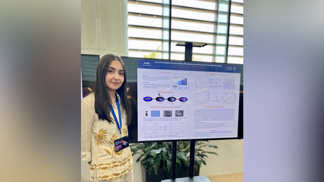
Anwar Alshaibani

Nanbo Li
Jonathan Klein


Karen Sanchez
Hani A. Al Majed


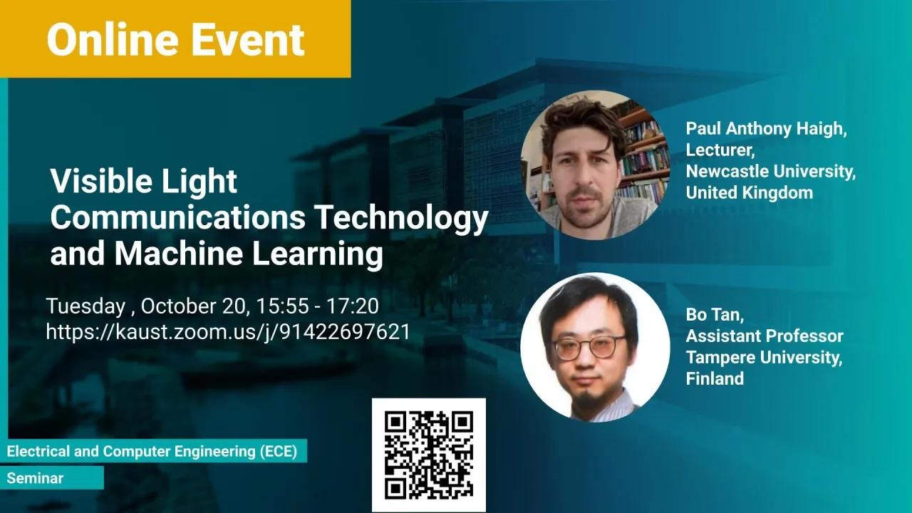
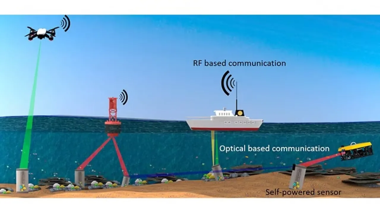
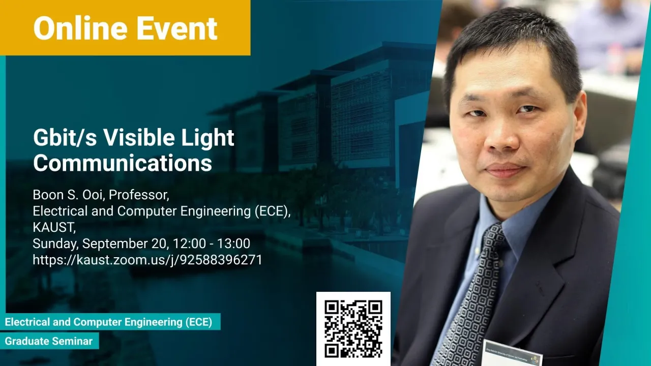
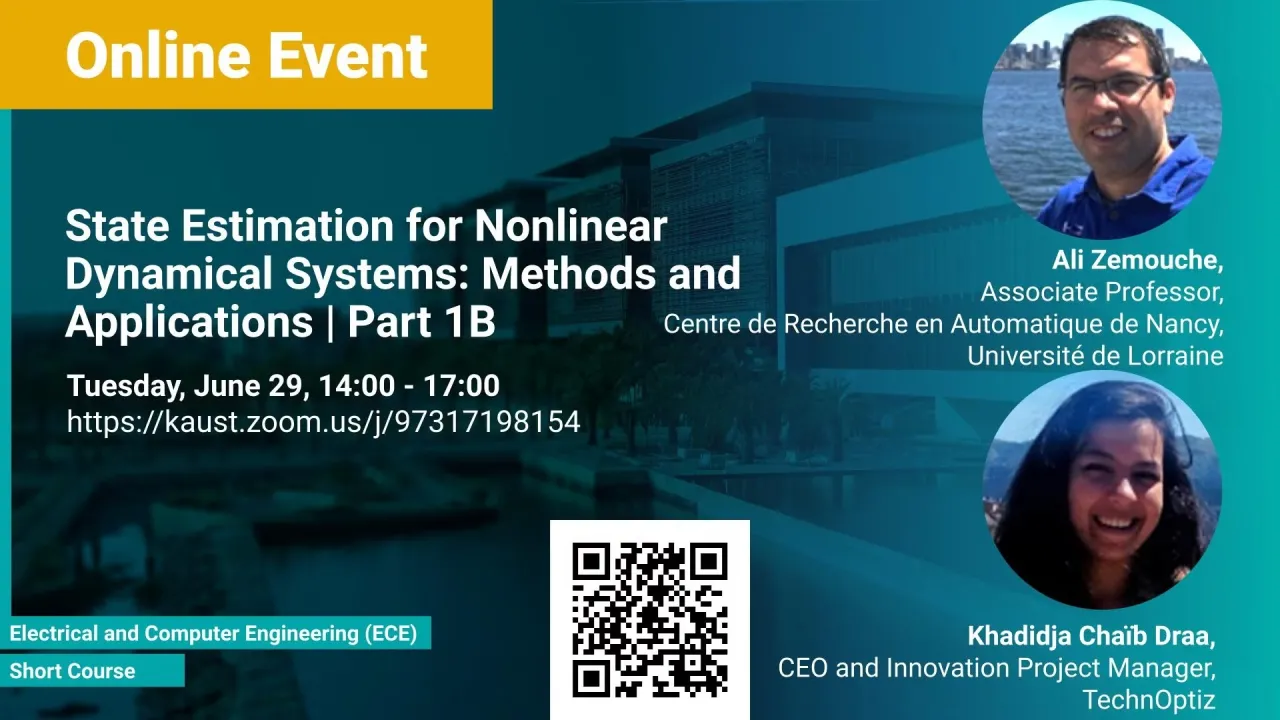
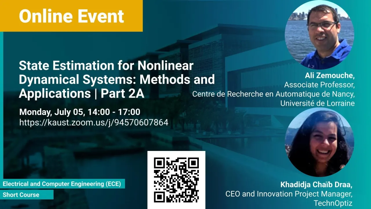
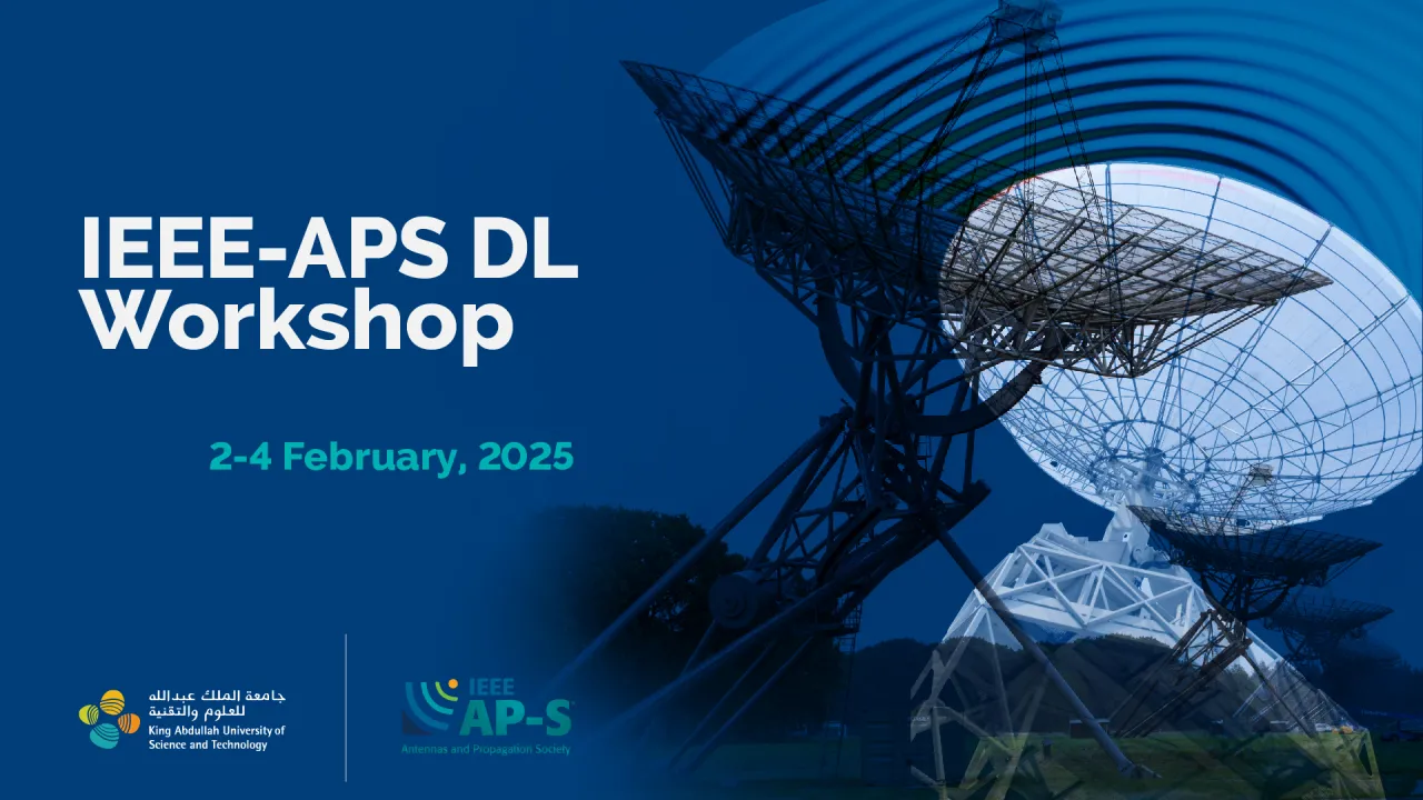
Visible Light Communications Technology and Machine Learning - 2020-10-20
Paul Anthony Haigh, Newcastle University, United Kingdom and Dr. Bo Tan, Tampere University, Finland
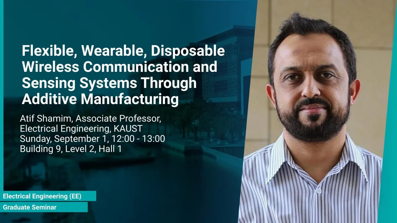
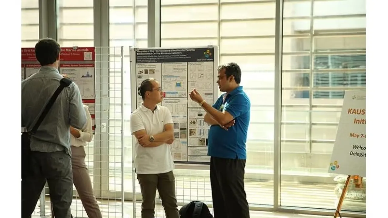
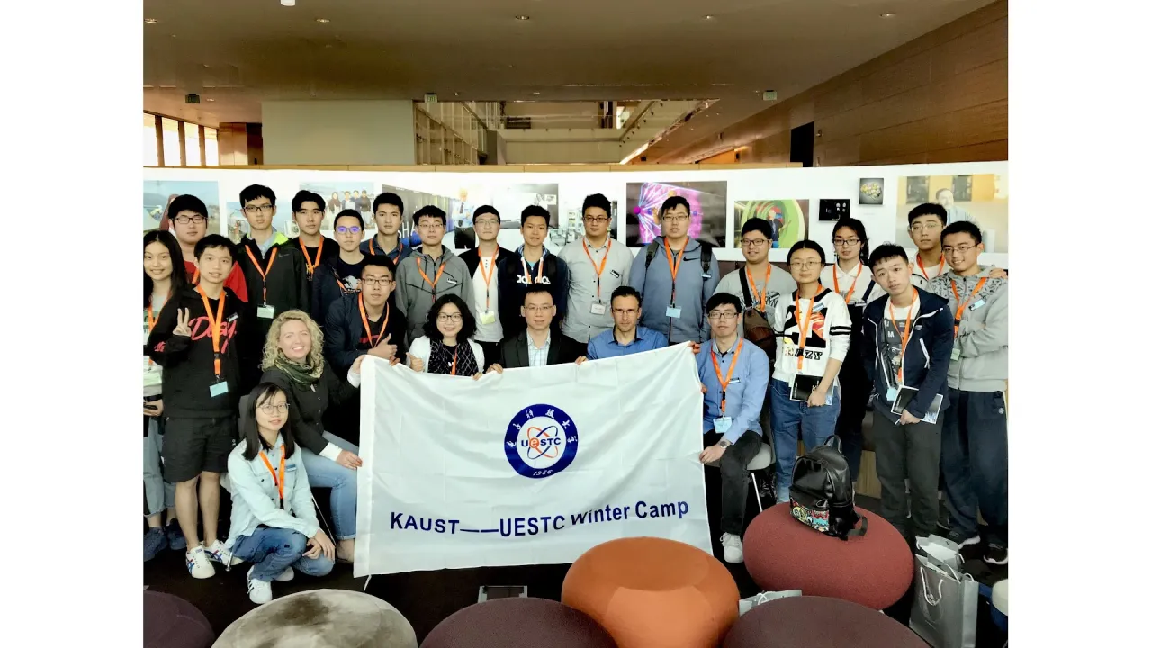
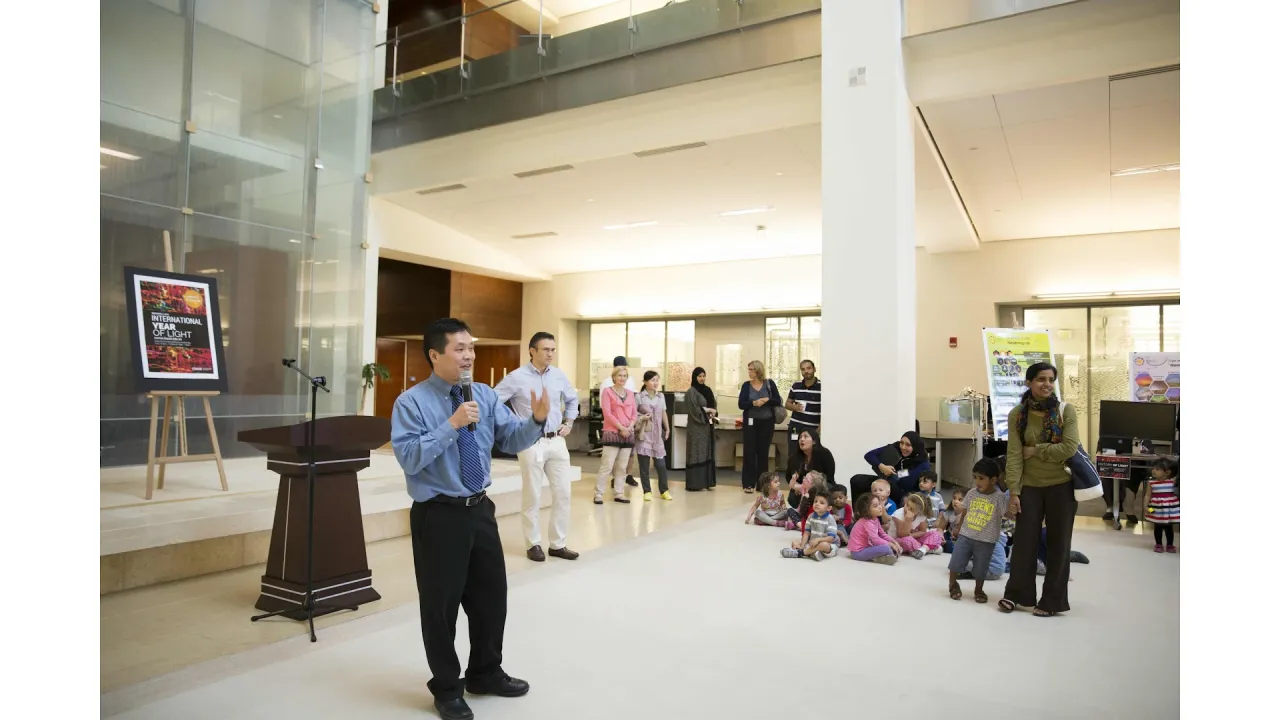
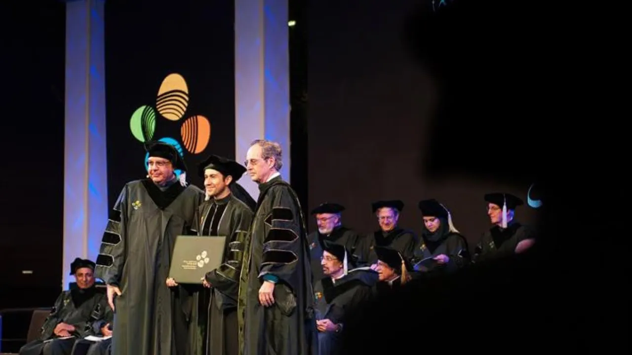
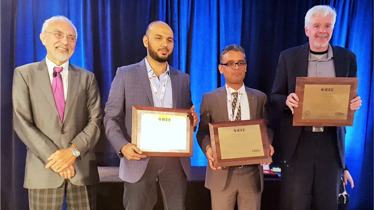
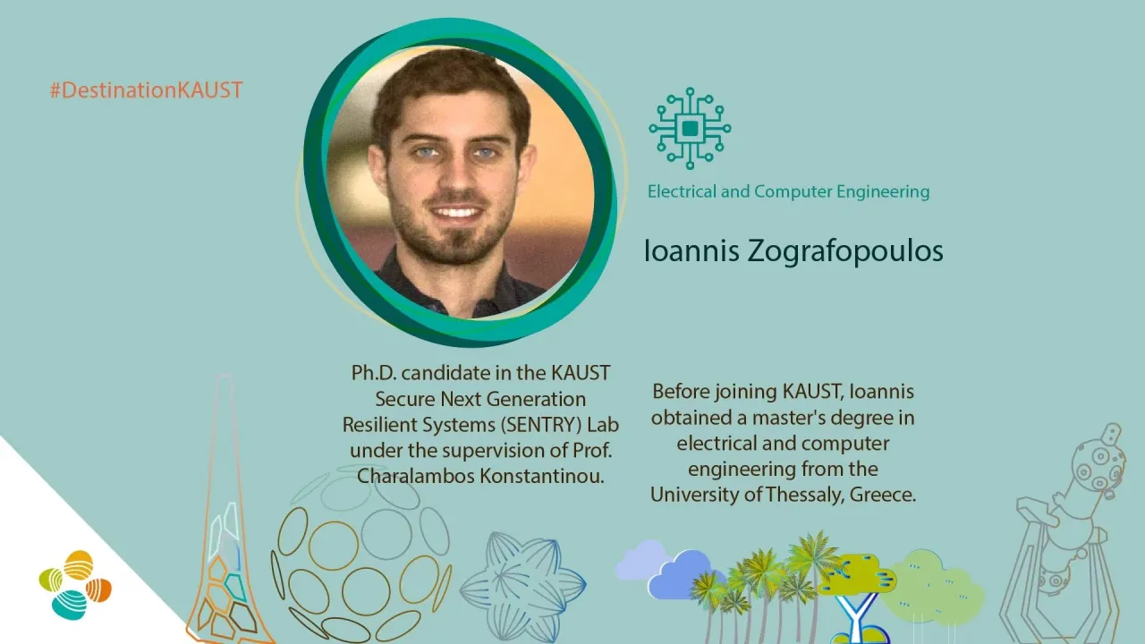
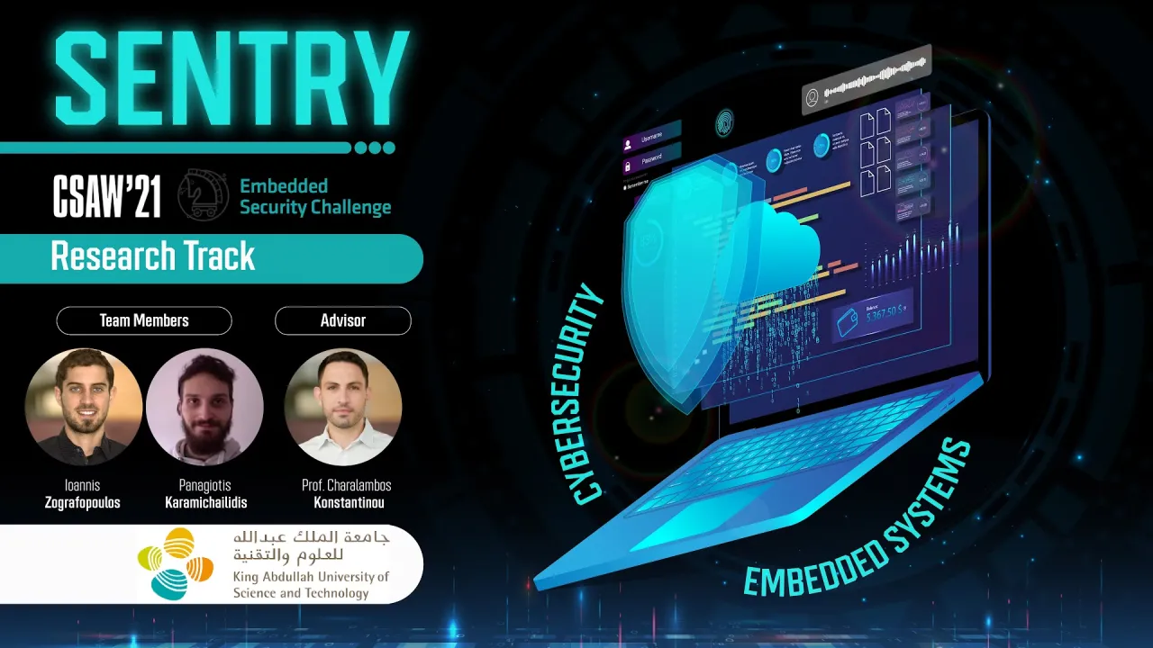
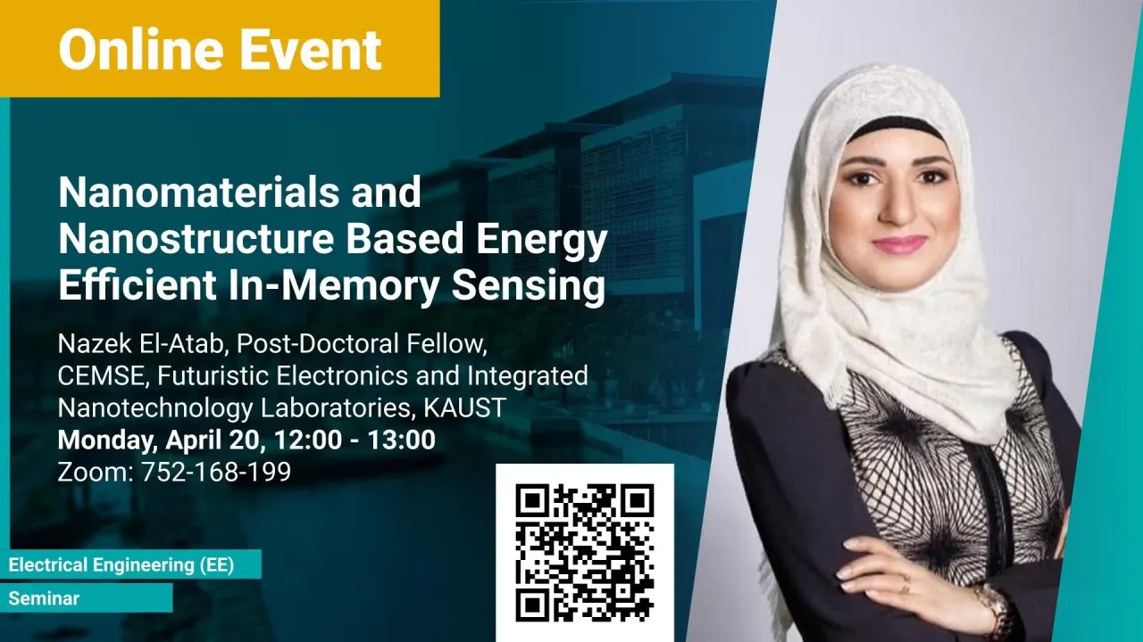
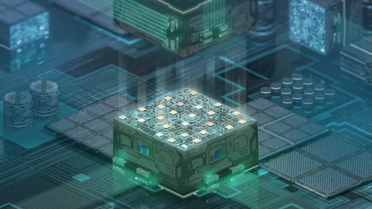
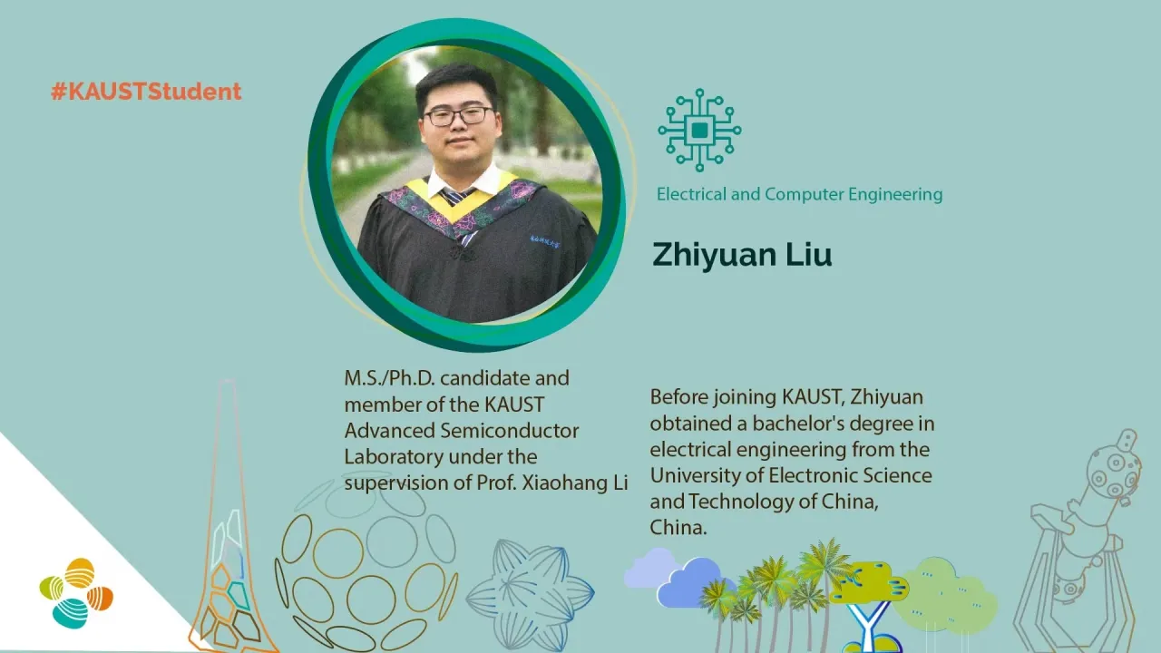
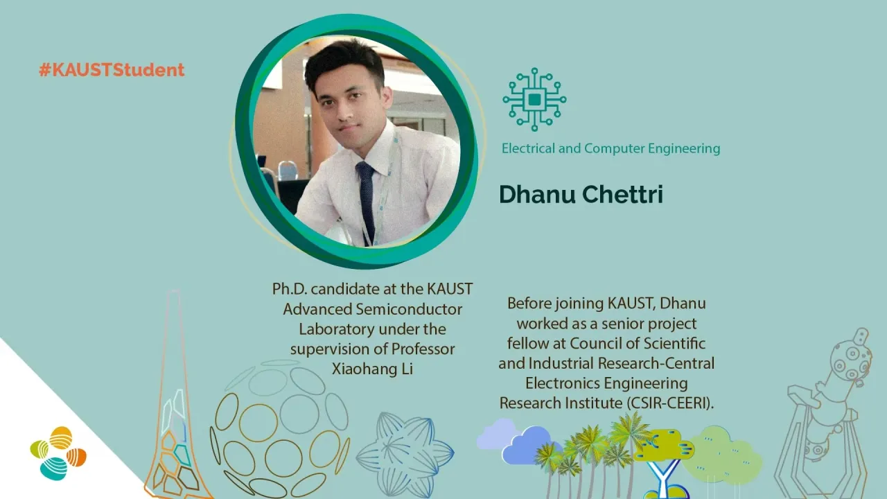
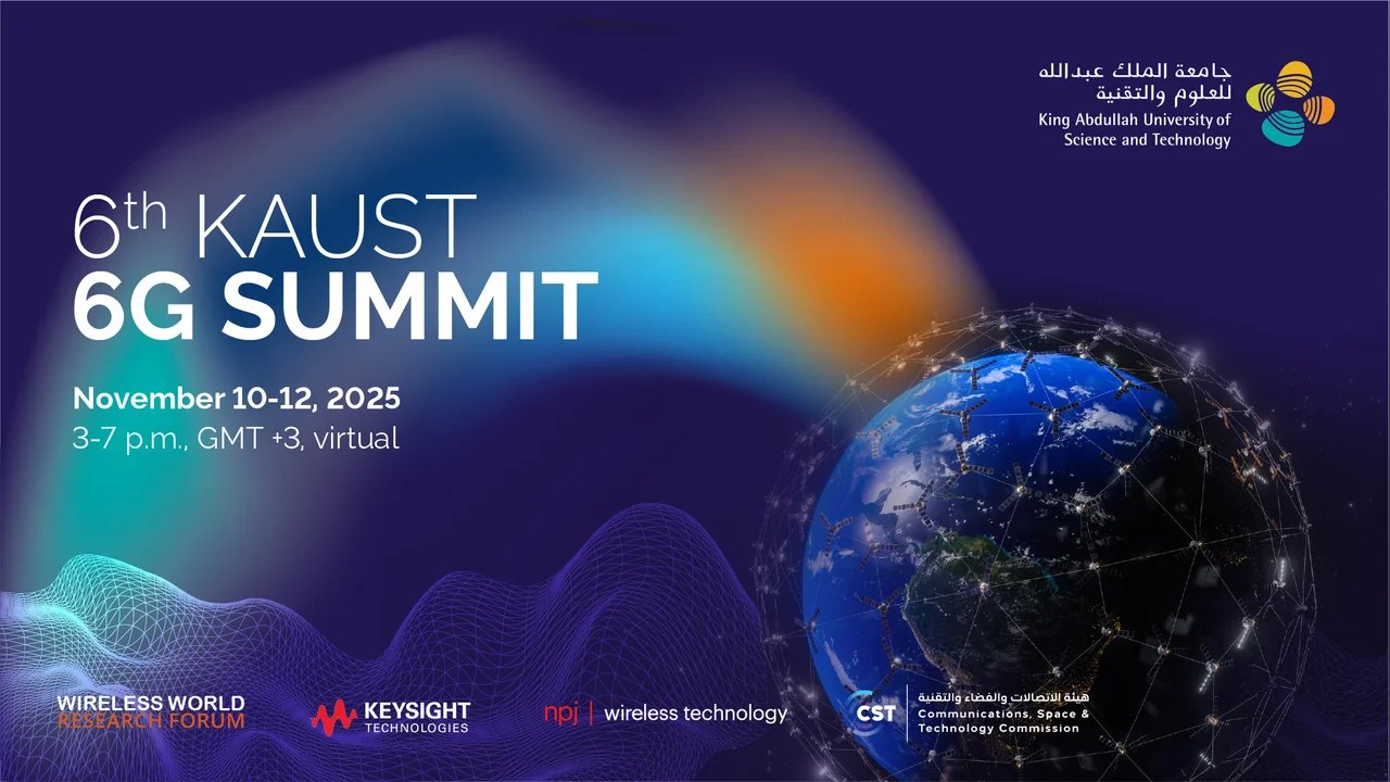
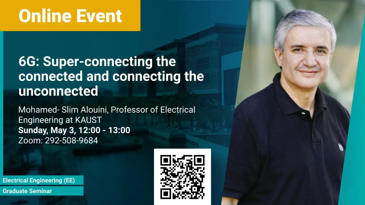
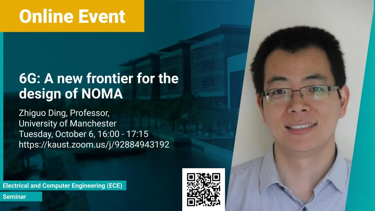
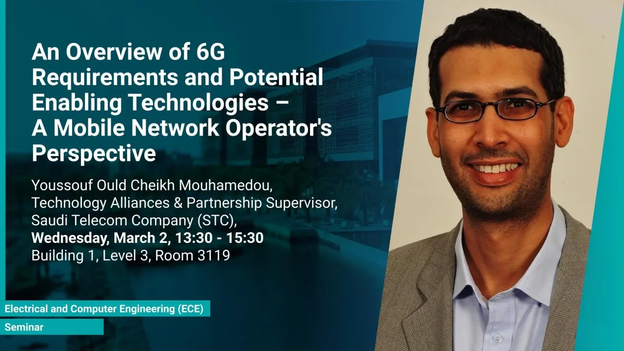
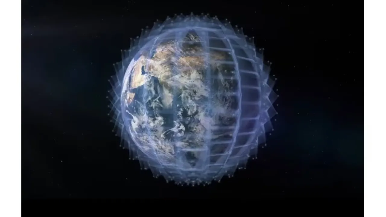
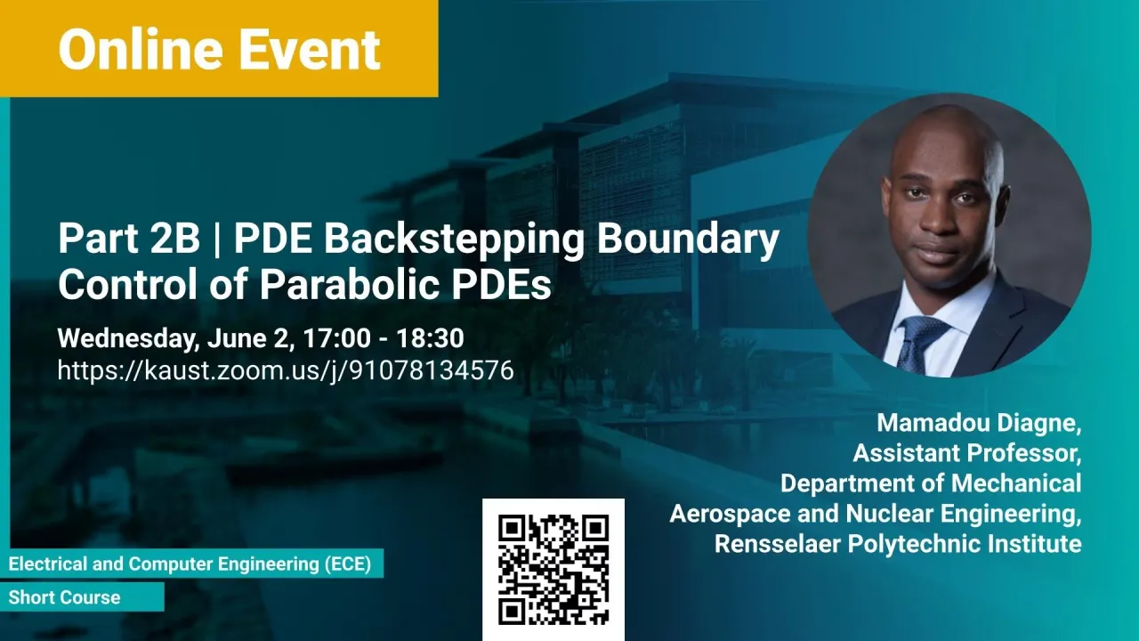
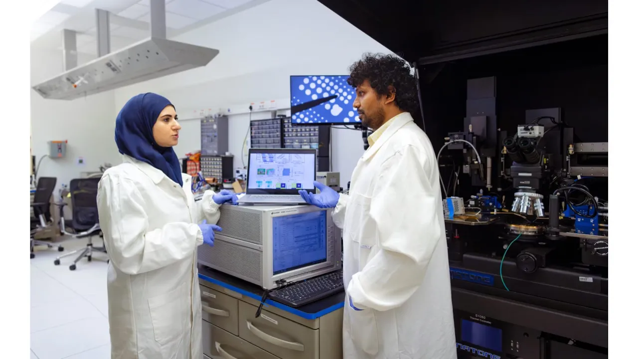
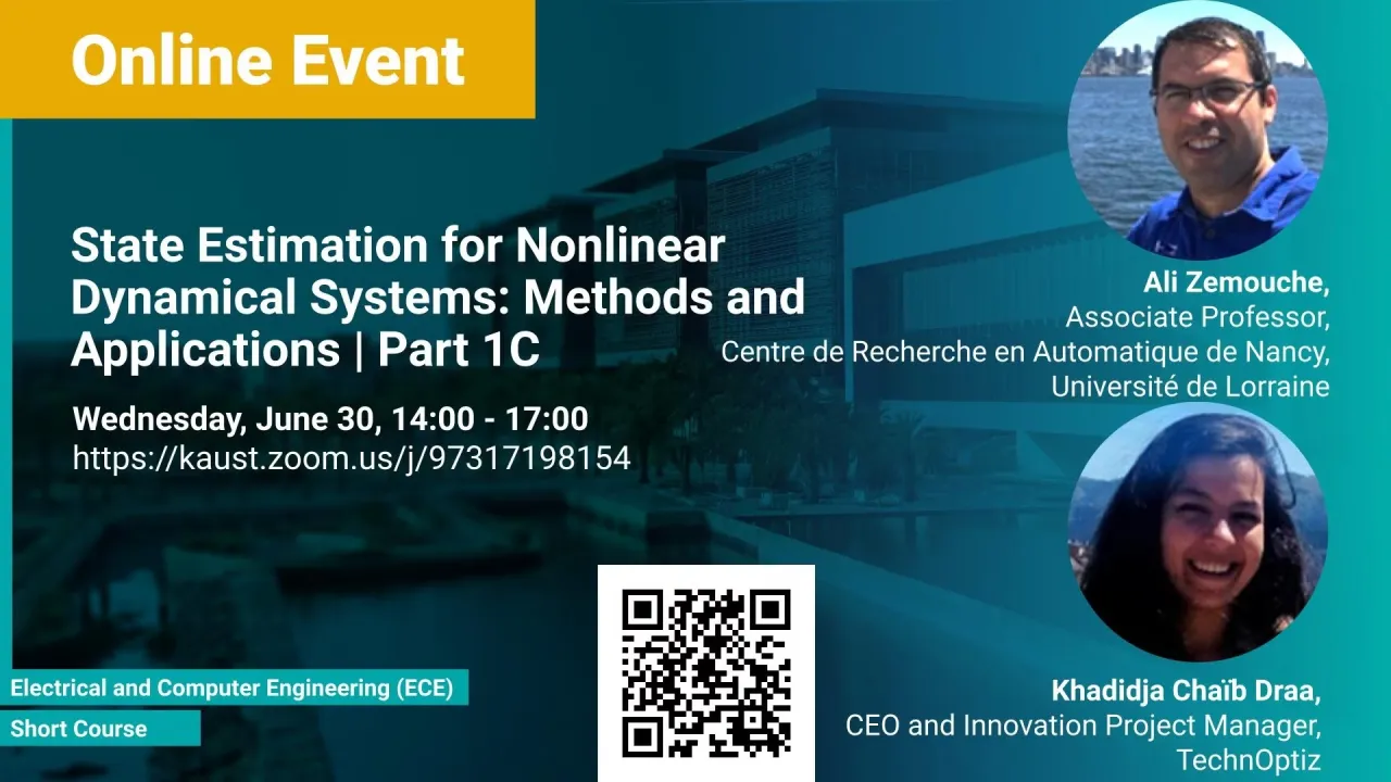
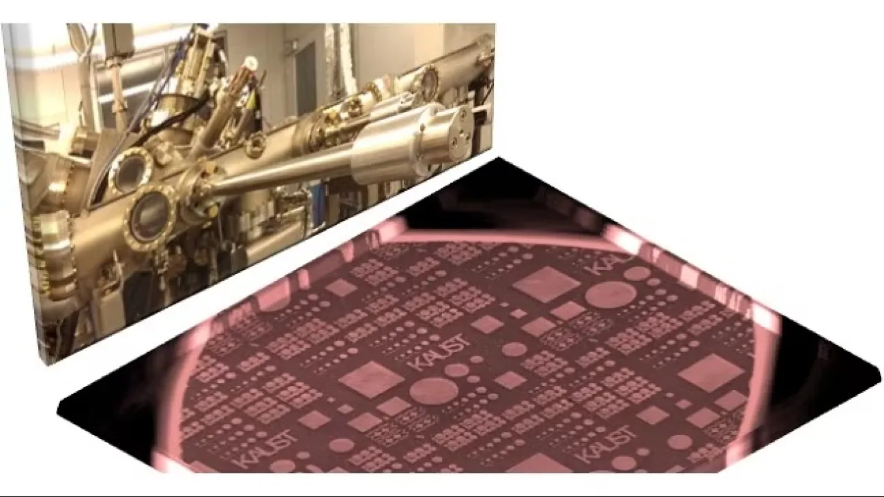
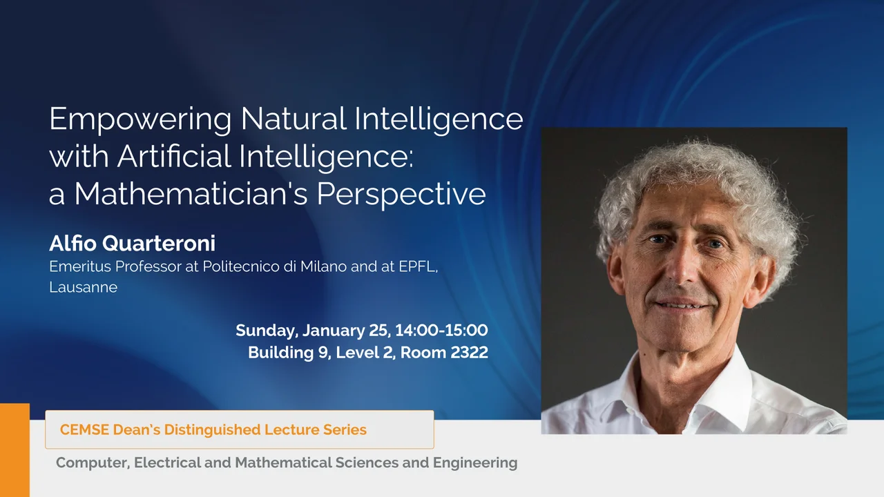
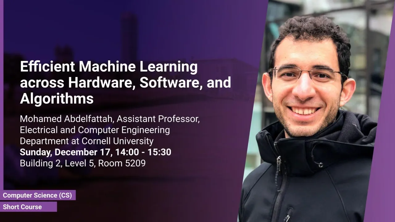
KAUST
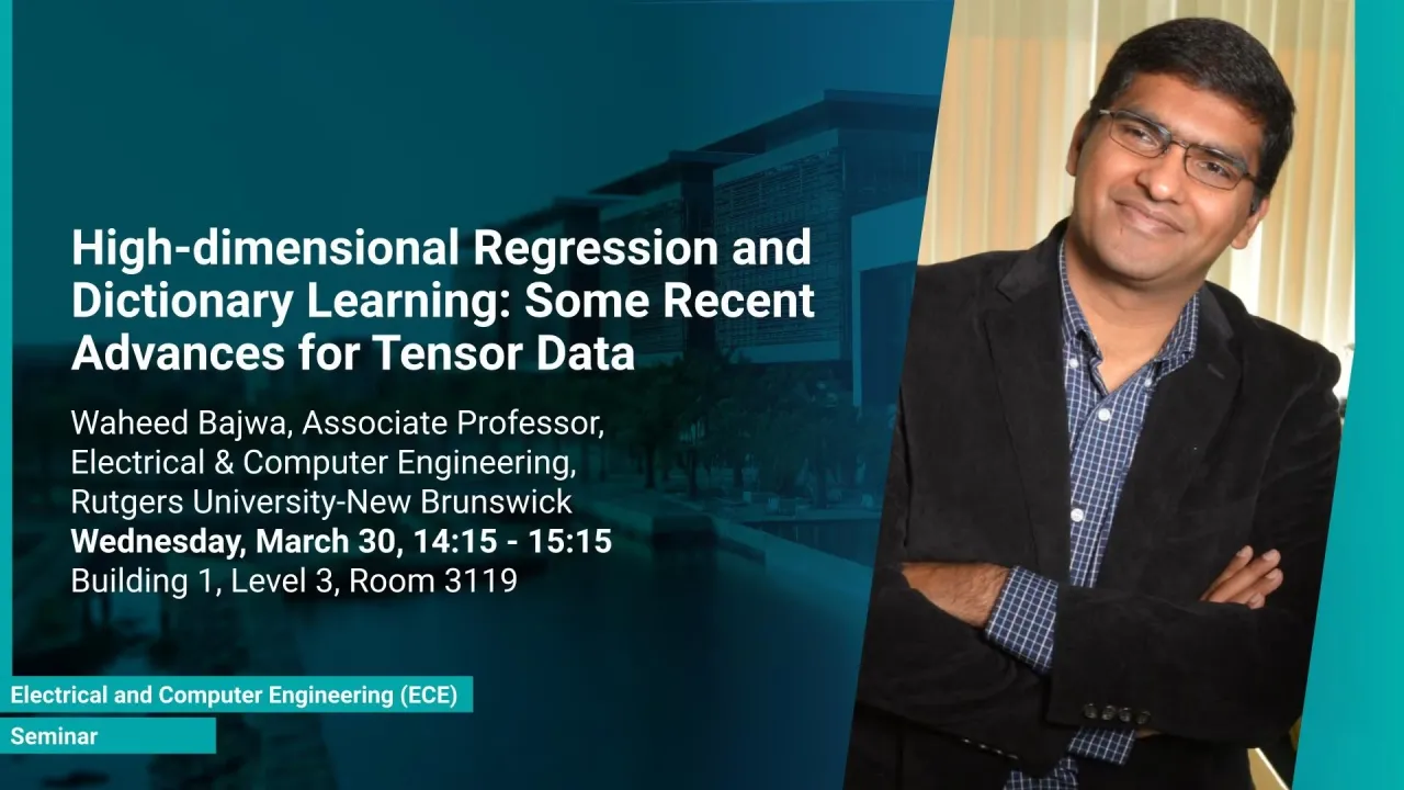
High-dimensional Regression and Dictionary Learning: Some Recent Advances for Tensor Data
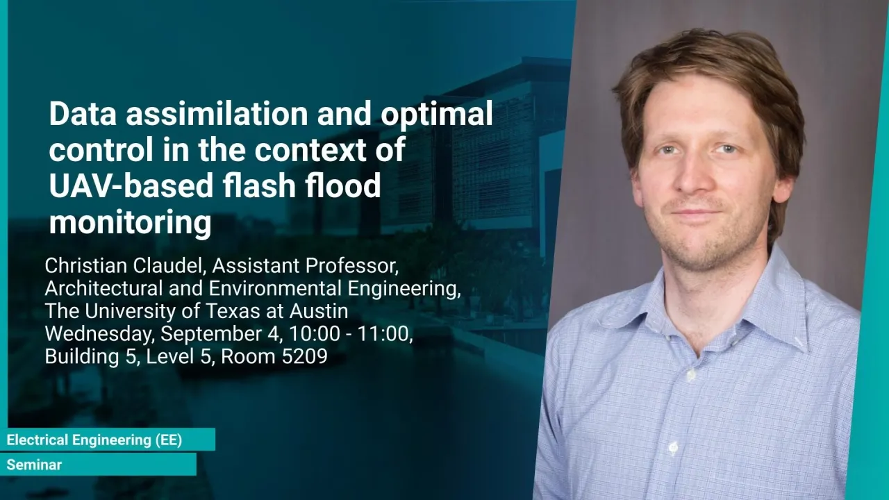
Prof. Waheed Bajwa, Electrical and Computer Engineering, Rutgers University-New Brunswick
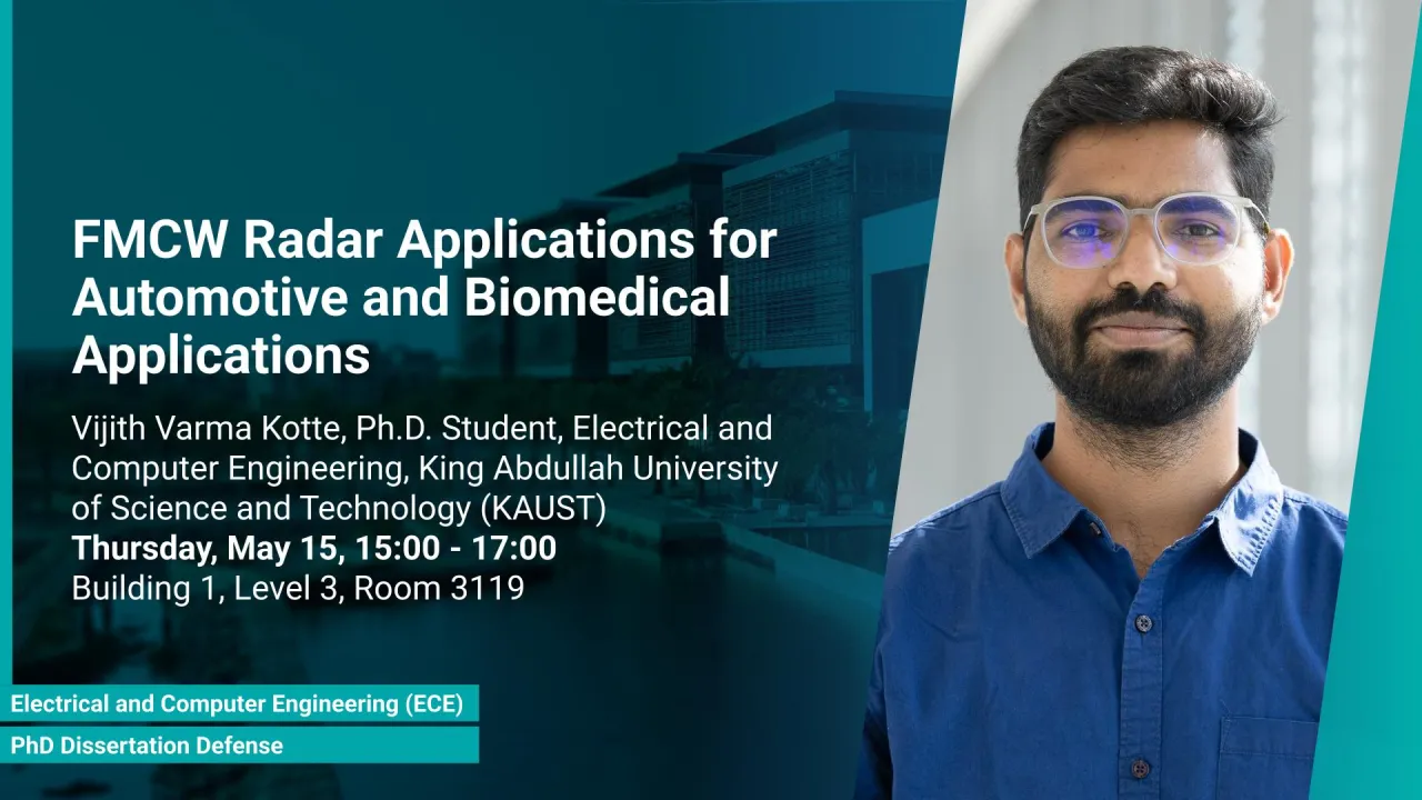
B1 L3 R3119
Machine Learning for Biomedical Engineering: from Oncological Electroporation to Gesture Recognition
Luciano Tarricone, Department of Innovation Engineering, University of Salento
B9 L2 H2
Machine-learning-assisted Quality of Transmission Estimation in Optical Networks
Andrea Bianco, Full Professor, Electronics and Telecommunications Department at Politecnico di Torino
B9 L4 R4125
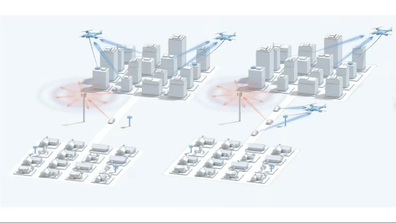
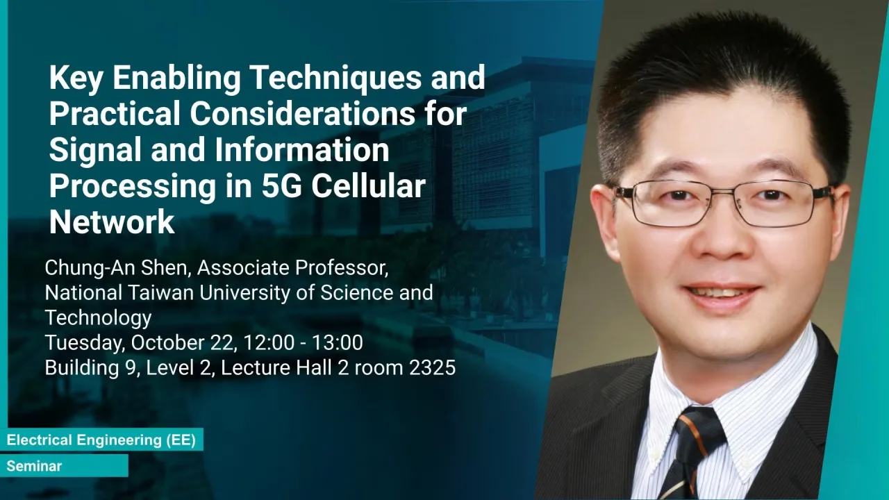
Machine Learning for Scalable MIMO Communication Systems: From Theory to Real-World Demonstration
Dr. Ahmed Alkhateeb, Electrical Engineering , Arizona State University
B9 L2 H1
Yibo Yang
Waleed Abu Laban
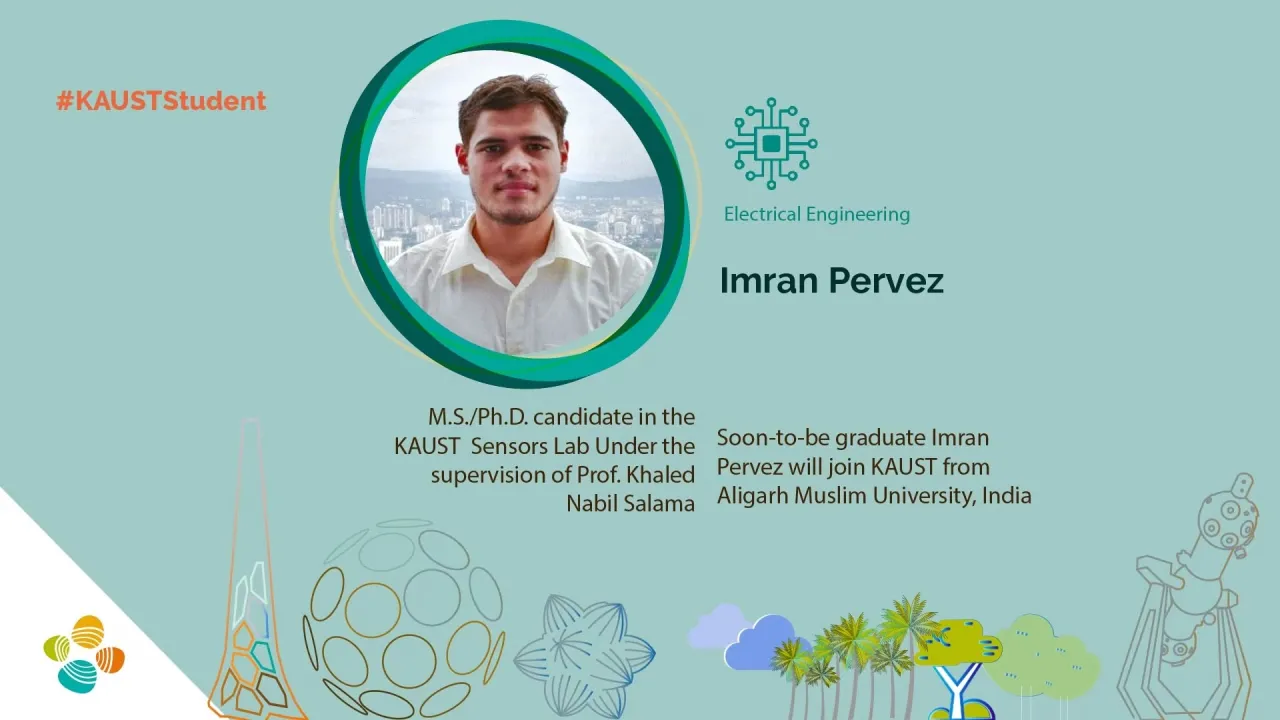
Mostafa Mohamed Lotfy Emara
Mohammed Aldosari
Maria Sara Nour SADOUN

Lin Chen
Lama Burhan Niyazi
Kumail Alhamoud


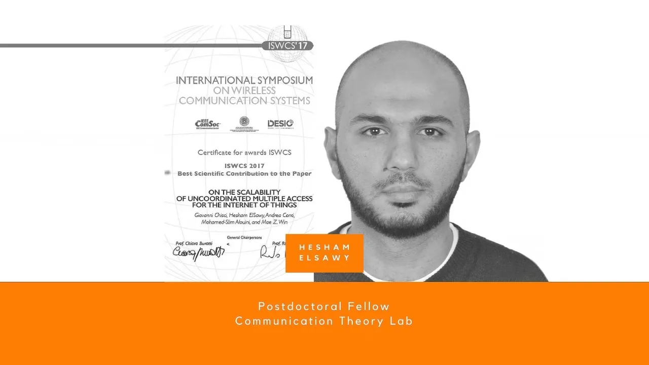
Islam Ashry
Hajar El Hammouti
Arman Ibrayeva
Abdullah Adil Albakry

Abdallah Al-Moubayed
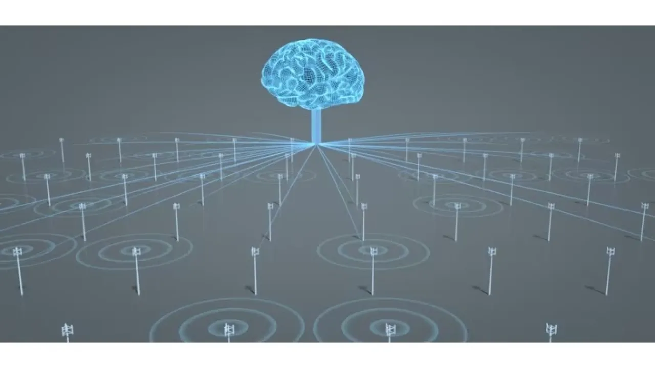
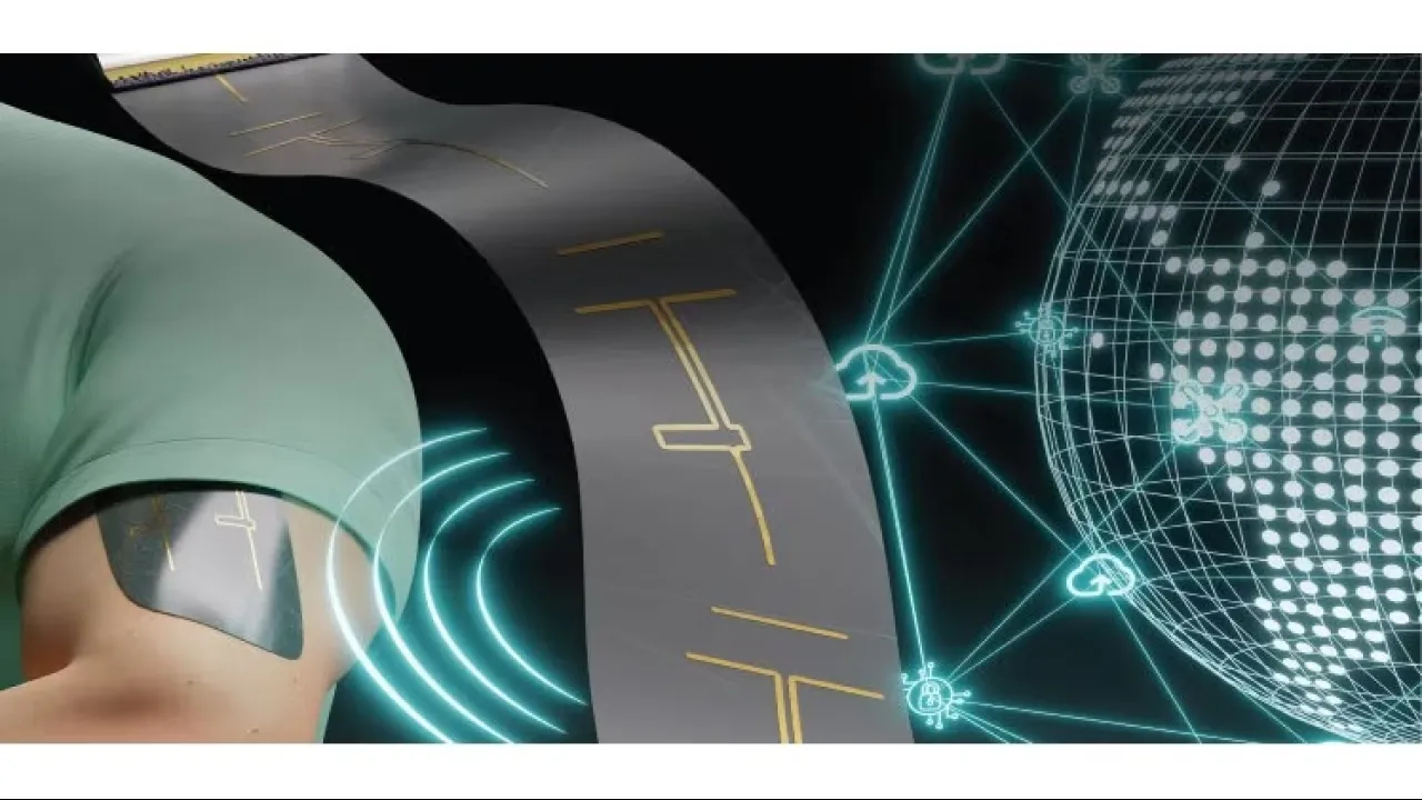
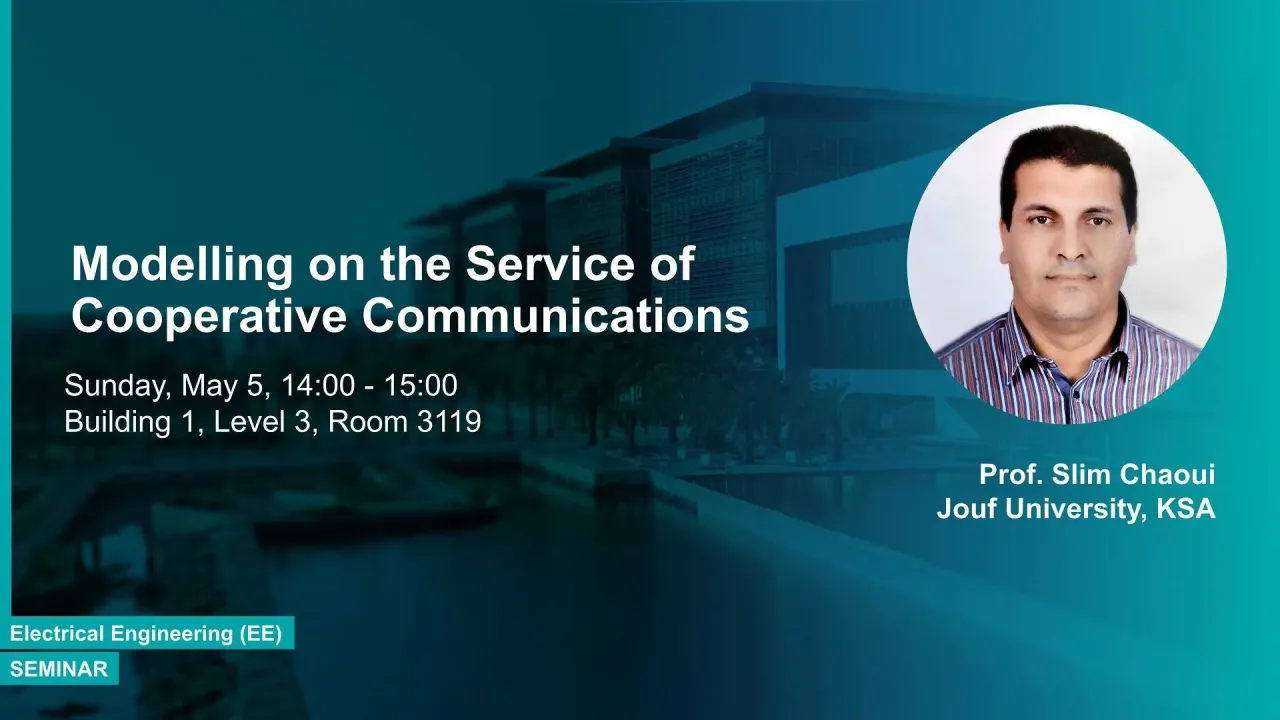
wireless communication Cross-layer design machine learning cybersecurity Data Analytics Resource allocation wireless resource virtualization Device-to-Device Communication IoT e-learning performance and optimization modeling cloud computing Cooperative communications Collaborative instantly decodable network coding